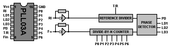
PLL03A and PLL08A
PLL frequency
synthesizer
Overview
This 27 MHz band, PLL
frequency synthesizer LSI chip is designed specifically for CB transceivers.
Programming Chart for
|
|
Channel |
RX |
TX |
|
1 |
1206 |
1297 |
|
2 |
1208 |
1299 |
|
.. |
.... |
.... |
|
22 |
1258 |
1349 |
|
.. |
.... |
.... |
|
40 |
1294 |
1385 |
NOTES:
- Special divided-by-2
circuit in TX mode change referency divider output to 2.5kHz steps.
- 91-count upshifts on TX
provides 455kHz offset for receiver IF mixing when VCO frequency is doubled.
- Since chip cannot
divide VCO directly, it is down-mixed with the 10.240 MHz referency
oscillator signal, producing
6 MHz outputs (RX Mode) and 3 MHz outputs (TX Mode) into dividers. Standard 16 MHz VCO is used. - PLL08A contains only
the first 22 FCC channels for EEC use, otherwise both chips are
identical.
Example of VCO determination, channel 1:
1206 x 5 kHz + 10.240 MHz = 16.270 MHz (RX-Mode)
1297 x 2.5 kHz + 10.240 MHz = 13.4825 MHz (TX-Mode)
(13.4825 MHz x 2 = 26.965 MHz)